Proposal for Radio Development for the Wireless Adaptable Network Node (WANN) Project, DARPA BAA 06-26
Executive Summary
This proposal is for development of radios for the Defense Advanced Research Projects Agency’s (DARPA) Broad Agency Announcement (BAA) 06-26, Wireless Adaptable Network Node (WANN). The WANN BAA specifically addresses the radio requirements for the communications system outlined in the DARPA BAA 05-50 Wireless Network after Next (WNaN). The thrust of WNaN is to replace high cost sparsely located communication devices with low cost flexible devices that are deployed on a massive scale and configure themselves into a functioning ad-hoc network. The radio requirements for WANN are presented below, as well as an outline for a technical solution.
The WNaN philosophy envisions a mobile ad-hoc network consisting of inexpensive network nodes. This network is to be based on the Open Systems Interconnection (OSI) layered model and is to pass IP traffic from end to end. The network nodes are to be self configuring into a flexible mesh network. Interfaces to the nodes will include Ethernet and Voice over IP (VoIP). They are also to be inexpensive with a maximum cost per node of $500. The radio and network requirements of WNaN are further described in the subsequent BAA’s WANN and WNaN Adaptive Network Development (WAND) respectively.
The WANN BAA outlines the desired radio characteristics for WNaN including frequencies, power requirements, throughput, Quality of Service (QoS), and OSI layer one and two networking requirements. WANN radios are also supposed to incorporate or be compatible with several existing and DARPA defined technologies: Multiple Input Multiple Output (MIMO), Mobile networked MIMO (MnM), Control Based Mobile Ad hoc Networks (CBMANET), Micro-Electro-Mechanical Systems (MEMS) filters, and Dynamic Spectrum Use (XG).
This proposal presents a technical solution for the DARPA BAA 06-26 WANN radio utilizing chip sets designed for IEEE 802.16 also known as WiMAX. The BAA stipulates that the radios be built from commercial off the shelf integrated circuits and that they be inexpensive. The Texas Instruments chip set used in this proposal satisfies these requirements.
Both Digital Signal Processing (DSP) and hardware development are defined in this proposal. In general, DSP and hardware development follow separate tracks, however, some key milestones require success of both simultaneously. A phased approach is used so that each phase can be evaluated as completed, and possible adjustments to this proposal can be considered. This provides some flexibility as design and implementation problems are encountered. A schedule and list of milestones are provided.
Technical Proposal
WANN Requirements
WANN radio frequencies are specified to be between 900MHz and 6GHz. One interpretation of this specification is that the unlicensed Industrial Scientific and Medical (ISM), with frequency bands in this frequency range, should be used. The ISM bands include the spectrum between 902-928 MHz, 2.400-2.500 GHz and 5.725-5.875 GHz. WANN also specifies that the radios be built with Commercial Off The Shelf (COTS) integrated circuits. A survey of COTS radio frequency integrated circuits reveals that multi band chips are available for frequencies that either include frequency bands of 900 MHz and 2.5 GHz or include the 2.5 GHz and 5.8 GHz frequency bands. The solution presented here utilizes the 2.5 GHz and 5.8 GHz bands.
Although not specifically mentioned in the WANN BAA, Orthogonal Frequency Division Multiplexing (OFDM) provides high throughput and is the modulation method used in this solution. OFDM utilizes the Inverse Fast Fourier Transform to multiplex the input signals together. This means that only a single oscillator is required to transmit the composite signal. A Fast Fourier Transform is performed at the receiving end to retrieve the individual signals. The adjacent signals are also mathematically orthogonal. Since their cross product is zero, they can be placed next to each other in the frequency domain, so that no guard band is needed between them. OFDM was used in the prototype radios described in the DARPA sponsored paper An Adaptive Broadband Mobile Ad-Hoc Radio Backbone System.
Multiple Input Multiple Output (MIMO) technology is specifically mentioned in the WANN BAA. MIMO uses multiple transmit and receive antennas to improve signal throughput. There are two type of MIMO. One type uses the multiple transmit paths to transmit the same signal and combine the results at the receiver. The other method actually uses spatial diversity to send separate signals on the same frequency.
Another consideration for the devices chosen for the radios is that they will pass IP traffic and use protocols based on the OSI model. The network nodes are to configure themselves into a mesh network that provides an end to end IP network. The VoIP requirement necessitates some type of QoS provisioning.
Several chip sets designed for wireless LAN (WLAN) applications were considered for this proposal. The approach presented here is to use an existing technology and modify it rather than to build a solution from scratch. The pending IEEE 802.11n provides for operation in the 2.5 GHz and 5.8 GHz bands and provides for OFDM and MIMO. The problem in implementing this solution, however, is that the PHY and MAC protocols are pre programmed into the base band chip for 802.11n operation. Another factor is that the 802.11n market is extremely competitive at present. This poses at least two concerns. One is that the chip manufacturers are somewhat secretive about the technical details of their products, lest a competitor glean information for development of their own products. Second, since the competitive market is so volatile, a selected vendor may be bought out or go out of business, which could effect availability of the devices. For these reason, an IEEE 802.16 chip set was chosen for this proposal.
Technical Approach
Design
Texas Instruments provides a dual band 802.16 chipset that we are proposing for the WANN radio. This solution has a higher chip count than some other wireless technologies, however, it is also much more flexible and allows the development necessary to satisfy the WANN requirements. One advantage to this solution is that these devices are commercially available from multiple suppliers. Also, Texas Instruments provides detailed datasheets and development information on their web site. An implementation of this chip set is shown below.
TRF2436 TRF2432 TMS320C6713 GC1115 GC5016
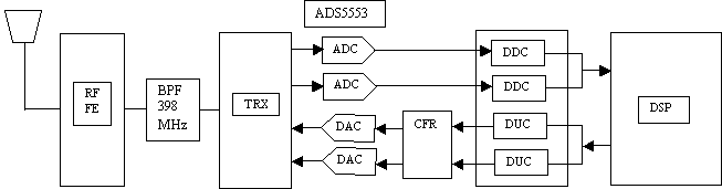
The TMS320C6713 Digital Signal Processor (DSP) performs layer 1 and layer 2 processing and creates the digital signal to be transmitted. The GC5016 then performs a base-band to pass-band conversion. The GC5016 is a crest factor reduction processor that essentially reduces peaks in the output signal to improve the efficiency of the follow on power amplifiers. Next, the ADS 5553 performs the digital to analog signal conversion. The signal then passes to the TRF2432 dual band transceiver that modulates the IF carriers and passes the signal to the TRF2436 dual band RF front end for transmission at 2.5 and 5.8 GHz. The received signal basically goes through the reverse process and the transmitted information is recovered by the DSP. For MIMO operation, an additional TRF2436 RF front end is need for each channel at a minimum, depending on the type of MIMO employed. Note also that additional interface circuitry is needed to connect Ethernet and other interfaces to the DSP.
This design provides the flexibility necessary for development of the WANN radio. These devices are readily available from multiple vendors and since the technology is more established than the 802.11n, the future availability is more certain. The flexibility of this design also allows for incorporation of the WANN requirements of MnM, CBMANET, MEMS, and XG.
Development Procedure
The WANN radio development will be accomplished in three phases. Phase I DSP development includes development of base-band algorithms using MATLAB. These algorithms will then be used to program the DSP. The purpose of this is to demonstrate successful operation of the DSP, and to provide a signal to the uplink converter, digital to analog converter, transceiver and RF front end. Phase I RF development will utilize TI supplied evaluation boards to provide a baseline design reference. Success of Phase I RF is defined as detectable transmission of the signal provided by the DSP. After successful completion of Phase I, the design of the printed circuit board for the radio will begin for Phase II RF. Since these will be four layer boards, they will need to be fabricated by an outside vendor. Phase II DSP development will entail development of OFDM algorithms using MATLAB. The DSP will then be programmed to produce an OFDM signal for transmission. Success of Phase II is defined as end to end transmission between a transmitter and receiver. Phase III entails development of Layer 1, layer 2 operation and Ethernet interfaces.
Schedule
January February March April
Task 5 12 19 26 2 9 16 23 1 8 15 22 29 5 12 19
Phase 1 DSP development ------------
Phase 1 RF development ---------------------
Phase II DSP development --------------------------
Phase II RF development --------------------------
Phase III DSP development ------------
Pahse III Hardware development -----------
Report Generation --------------------------------------
Milestones
The following milestones present a method of tracking project progress.
1. Successful baseband DSP operation (Phase I).
2. RF Transmission of DSP signal via radio built with development kits (Phase I).
3. Successful OFDM baseband DSP generated signal (Phase II).
4. Successful radio RF output (Phase II)
5. Successful OFDM RF output from radio (Phase II).
6. Successful end to end connectivity between transmitter and receiver (Phase II).
7. Successful Layer 1 and layer 2 DSP programming (Phase III).
8. Successful test of Ethernet and VoIP interfaces (Phase III).
Deliverables
The following deliverables are specified for this proposal.
1. Final Report including the following:
Detailed design documentation
DSP programming code
Implementation narrative
Test results for milestones listed above
2. Progress reports at each milestone to include any request for proposal modification.
Key Personnel
The principal investigator for this project is William F. Rideout.
Previous Experience
Mr. Rideout is currently pursuing a MSEE degree from Capitol College in Laurel, MD with an anticipated graduation date of May 2008. He has taken classes there that include digital signal processing using MATLAB and circuit design using SPICE. Also, he is currently enrolled in a microwave class. His BSEE is from Virginia Tech, Blacksburg, VA in 1983. He has 20 years experience in the telecommunications industry including OSI layered networking technologies and various programming tasks. He has many years of experience designing and assembling electronic projects.
Project Costs
|
Materials |
|
|
|
|
|
Description |
Part
No |
Quantity |
Cost |
Total |
|
RF Front
End |
TRF2436 |
3 |
$15.00 |
$45.00 |
|
RFFE Eval
Board |
TRF2436EVM |
1 |
$299.00 |
$299.00 |
|
IF
Tranceiver |
TRF2432 |
3 |
$10.00 |
$30.00 |
|
TXR Eval
Board |
TRF2432EVM |
1 |
$299.00 |
$299.00 |
|
Analog to
Digital Converter |
ADS5232 |
3 |
$24.00 |
$72.00 |
|
Digital
to Analog Converter |
DAC56x2
5686/7 |
4 |
$30.00 |
$120.00 |
|
CFR |
GC1115 |
3 |
$52.00 |
$156.00 |
|
Digital
Down/Up Converter |
GC5016 |
3 |
$43.00 |
$129.00 |
|
Down/Up
conv Eval Board |
GC5016EVM |
1 |
$199.00 |
$199.00 |
|
DSP |
TMS320C6711 |
3 |
$26.00 |
$78.00 |
|
DSP
Starter Kit |
TMDSDSK6713 |
1 |
$470.00 |
$470.00 |
|
CDC |
CDC7005 |
3 |
$15.00 |
$45.00 |
|
PC Boards
(qty1 is 3 boards) |
|
1 |
$219.00 |
$219.00 |
|
Handheld
6GHz Spectrum analyzer |
Spectran
HF-4060 |
1 |
$599.00 |
$599.00 |
|
Misc
parts |
|
1 |
$200.00 |
$200.00 |
|
|
|
|
|
|
|
Total
Materials |
|
|
|
$2,960.00 |
|
|
|
|
|
|
|
Labor |
|
|
|
|
|
Description |
Personnel |
Hrs |
Rate |
Total |
|
Engineer
Level 5 |
William
Rideout |
400 |
$150.00 |
$60,000.00 |
|
|
|
|
|
|
|
Total
Cost Materials & Labor |
|
|
|
$62,960.00 |