DSP Implementation of a
Broadcast-band Software-defined AM Radio
By William F. Rideout
Report for
Master’s Project
For
Masters
Degree in
Electrical
Engineering
April 2008
Capitol
College
11301
Springfield Road
Laurel,
Maryland
A working software-defined AM radio is realized by use of a Texas Instruments (TI) TMS320C6713 Digital Signal Processor (DSP). The TMS320C6713 DSP Starter Kit (DSK) is used to implement the DSP and a TI ADS7881 analog to digital converter is used to sample the incoming AM signal. A simple envelope detector is used for the demodulation of the AM signal. Initially, an audio frequency AM test signal is generated by a computer sound card and demodulated by the DSP. Then, an actual broadcast AM signal is detected and heard from the DSK’s Codec through amplified speakers.
Table of Contents
Software-defined AM Broadcast Radio Development
End-to-End Operation of the ADS7881 – ‘C6713
Configuration
AM Rectification at 48 Kilo Samples Per Second (KSPS)
Antenna Installation and Signal recovery
Realization of the Working AM Broadcast DSP Radio
Appendix A - Code
Composer Studio Screen Shots
Appendix B – MATLAB Screen Shots
Appendix C – Listings of AM_Radio.c, functions.c, and
lp10k.h
Appendix D – Evolution of Interrupt Service Routines
Acknowledgements
I would like to acknowledge Professor Daniel Jablonski for his help and support enabling me to complete this project.
Introduction
I designed and built a software-defined AM radio detector that takes a broadcast signal from an antenna and produces an output audio that can be heard and recognized. Initially, I planned to have a software tuner as well as different examples of demodulators. As I got into the project, many challenges arose and I just concentrated on getting a working radio. As it turns out, there is a 20,000 watt AM station that broadcasts about 3 miles from my house that provides a good strong signal to work with, allowing me to demonstrate the demodulation without a tuner.
The operation of the radio involves conditioning the incoming AM signal so that it has a voltage level within the range of an Analog to Digital Converter (ADC), sampling the AM signal with the ADC, performing the demodulation in software running on the DSP, performing a Digital to Analog Conversion (DAC), and finally amplifying the audio signal and playing it through speakers. A block diagram of the AM radio is shown in Figure 1.
![]()
![]()
Speakers
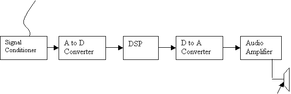
Figure 1 – Block Diagram of Software-defined AM Radio
A brief summary of the project development procedure is listed here.
1. Choosing a DSP and ADC.
2. Getting the DSP up and running.
3. Interfacing the ADC to the DSP.
4. Rectifying an audio frequency AM signal
5. Rectifying a radio frequency AM signal.
6. Adding a lowpass filter to complete the demodulator
Principles of AM Radio
A broadcast AM signal can be represented mathematically by the following equation:
![]()
where
Ac is the amplitude of the carrier wave,
ka determines the modulation index,
m(t) is the message or modulating signal, and
![]() fc being the carrier frequency.
fc being the carrier frequency.
The modulation index is defined as ![]() . This determines the depth that the message signal modulates
the carrier. To maintain an undistorted message signal, this ratio must remain
less than one. A Microsoft excel spreadsheet can be used to demonstrate AM
modulation. The equation, AM signal =
. This determines the depth that the message signal modulates
the carrier. To maintain an undistorted message signal, this ratio must remain
less than one. A Microsoft excel spreadsheet can be used to demonstrate AM
modulation. The equation, AM signal = ![]() , was used to generate figures below. Figure 2 shows 50%
modulation, Figure 3 shows 100% modulation, and Figure 4 shows 150% modulation.
, was used to generate figures below. Figure 2 shows 50%
modulation, Figure 3 shows 100% modulation, and Figure 4 shows 150% modulation.

Figure 2 – AM Modulation at 50% Modulation. A 2000Hz carrier is modulated by a 100Hz message signal.
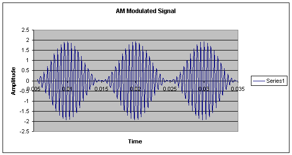
Figure 3 – AM Modulation at 100% Modulation. A 2000Hz carrier is modulated by a 100Hz message signal.
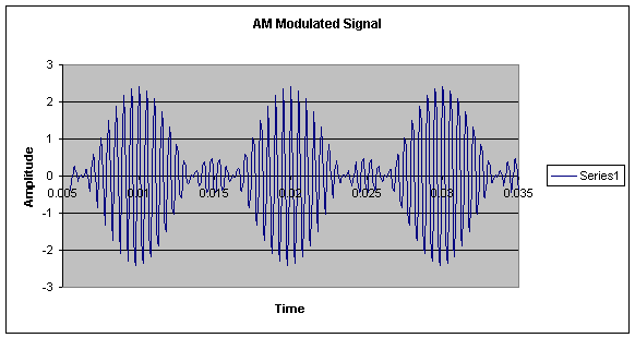
Figure 4 – AM Modulation at 150% Modulation. A 2000Hz carrier is modulated by a 100Hz message signal.
Note that when ka/Ac > 1, the envelope is distorted. This is an example of over modulation. When ka/Ac < 1, the carrier is said to be under modulated.
In general, there are two methods of demodulating an AM signal, coherent and noncoherent detection. Noncoherent detection does not use the frequency or phase of the carrier for detection. This method is commonly called envelope detection and can be achieved in hardware with a simple germanium diode and a low pass filter. Coherent detection requires mixing the AM signal with a signal that is the same frequency and phase as the carrier frequency. This is considerably more complex and typically utilizes Phase Lock Loop (PLL) circuitry.
For the SDR built in this project, a simple envelope detector is used. I used the absolute value function to “rectify” the AM signal and detect the message signal. This can also be modeled in excel as shown in Figure 5.
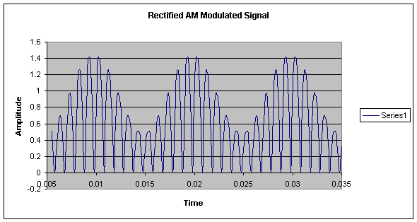
Figure 5 – Rectified AM Signal. The positive peaks of the carrier yield a signal that can be run through a lowpass filter to recover the message signal.
Software Defined Radio
A Software Defined Radio (SDR) is a radio in which functions, which are achieved by means of hardware in a conventional radio, are implemented in software. This may include mixing, filtering, demodulation, and amplification. SDR’s are becoming an important part of modern radio applications, as a single radio is required to use different modulation methods. A conventional radio requires duplicate hardware to achieve this, while an SDR simply needs to run different software. Also, evolving standards require different modulation algorithms for the same application. A conventional radio would most likely need to be replaced, while an SDR may just require a software upgrade.
The DSP demodulator in this project is a very basic example of an SDR. An SDR typically has an Analog to Digital Converter (ADC) to sample the incoming signal, a computer to run the software, and a Digital to Analog Converter (DAC) to create an analog output. An ideal SDR would input the incoming RF signal directly to the ADC, but existing ADC’s typically have a small dynamic range on their input so that an amplifier or other conditioning of the signal is required. In a practical SDR, an RF front end may also be required to select the carrier. Due to the limitations of ADC sampling rates, signals above 40MHz cannot be directly sampled and must use a direct conversion front end.
DSP and ADC Configuration
Equipment Selection
Choosing a DSP
I selected the Texas Instruments (TI) TMS320C6713 DSP for this project. The reasons for choosing this processor are that it is a powerful floating point DSP, it is available in a reasonably priced development kit, and there are many resources available for application development. The TMS320C6713 is commonly referred to as the ‘C6713, so I will do so here. The ‘C6713 is an affordable member of the TI TMX320C6000 DSP series. The DSP Starter Kit (DSK) can be purchased for $415 from Spectrum Digital at http://www.spectrumdigital.com./. The DSK includes the DSP, a 225MHz clock, an on board audio codec, and a USB interface that communicates with the DSP through an on board Joint Test Action Group (JTAG) interface. The on board audio codec is a TI TLV320AIC23; in the literature this is shortened to AIC23 as I will do in this document. It also comes with an Integrated Development Environment (IDE) Windows application called Code Composer Studio.
Choosing an Analog to Digital Converter
I chose the TI ADS7881 for the Analog to Digital Converter (ADC) that will sample the incoming AM signal and provide the digital input to the ‘C6713 DSP. I selected this ADC because of its 4 Mega Samples Per Second (MSPS) sampling capability and the fact that it can be purchased as part of an evaluation board that is made to interface with the ‘C6713 DSP. The evaluation board, including the ADS7881 cost $99 from Texas Instruments at http://www.ti.com/. For the AM broadcast spectrum, 540-1600 KHz, the Nyquist criteria for sampling at twice the highest frequency requires a sampling rate of 2 x 1600 KHz or 3.2 MSPS. The ADS7881’s sampling rate of 4MSPS can handle this. I chose a parallel interface because a serial interface would run operate around 40 MHz, which might prove difficult to work with. The evaluation module (EVM) with the ADS7881 installed is designed to interface with the ‘C6713 DSK via a 5-6K interface board.
5-6K Interface Board
This board provides a system development platform and access to the ‘C6713 DSK’s external memory and peripheral interfaces. I chose to get this because it provides a hardware interface between the ‘C6713 DSK and the ADS7881 EVM. It is called a 5-6K because it with both TI’s TMS320C5000 and TMS320C600 series DSKs. This board can be purchased from TI for $49. It also provides screw terminals to hook up the external supply voltages required by the ADS7881 EVM. A picture of my ‘C6713 DSK, 5-6K Interface board, and ADS7881 EVM is shown in Figure 6.
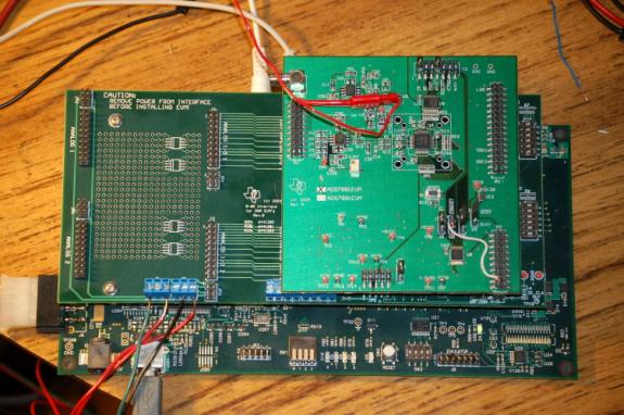
Figure 6 – The ‘C6713 DSK is shown on the bottom, the 5-6 K interface in the middle and the ADS7881 on top. The red lead clipped onto the ADS7881 EVM is the input from the antenna. The white jumper wire on the ADS7881 EVM provides the sample timing from the ‘C6713 to the ADS7881. On the 5-6K board; the green wire supplies –12Vdc, the red wire just to the right of it supplies +12Vdc and the red wire to the far right supplies +5Vdc, and the black wire is ground. The Molex connector on the left supplies +5Vdc to the ‘C6713 DSK. The 3mm jacks on top provide audio output from the AIC23 Codec. The gray USB cable provides the programming interface to the host computer.
Setting up the DSK
I made extensive use of the book, Digital Signal Processing and Applications with the C6713 and C6416, by Rulph Chassaing, in my quest to get the TI TMS320C6713 DSK up and running. I found this book on netlibrary.com, of which I have an account through my local Arlington, VA public library. I have found netlibrary.com to be a tremendous resource; it provides full reading access and has many good technical books. While I ended up buying this particular book, I had a chance to check it out, and with the price of textbooks, this was a great help
Code Composer Studio
The DSK comes with an IDE application called Code Composer Studio (CCS). CCS provides a C compiler and the software interface to the DSK board. It installed on my Windows XP system with no problem. Hardware interface from the computer running CCS to the DSK board is made via USB cable. One of the biggest problems I have encountered in getting projects to compile is getting the correct paths so that the CCS can find the files it needs. CCS creates a project file *.pjt for each new project. This text file specifies paths for source, library, and include files. Typically, sample programs will include the project file and source files to be built. I occasionally have modified these paths in the *.pjt file to get programs to compile. This should be done before the sample project is built for the first time, because some paths are embedded I binary files produced by the build process. In other words, if one was to do this, after and unsuccessful build, all the files should be deleted to start over. The –i path parameter can also be added to the build option string to identify the path for include files, I provide an example of this below.
Running a Program on the DSK
I made extensive use of the book, Digital Signal Processing and Applications with the C6713 and C6416, by Rulph Chassaing, to familiarize myself with the ‘C6713 DSK.
I describe here some additions and modifications to the projects that are included with the book to get them to compile. The book states that CCS version 2.x was used to develop the included programs. My DSK came with CCS version 3.1, perhaps this caused the problem. The book does explain that in order to run programs some additional files that did not come with the CCS had to be added to the projects. The following files are included on the CD that comes with the book, but initially, when I was using netlibrary.com, I found listings for them by searching the Internet as many college courses have used this book and provide the file listings for students. A brief description is given here:
C6713dskinit.h and C6713dskinit.c – header and sources file used to initialize the DSK, codec, and serial ports. I used these files in my AM_Radio project.
dsk6713_aic23.h – This header file provides parameters for the codec. I have also used this file in my AM_Radio Project.
The initialization and configuration performed by the functions in these files is straightforward and well documented in TI’s TMS320C6000 Peripherals Reference Guide and elsewhere. I would like to have built similar files from scratch, but wanted to stay focused on building a working radio.
The next two files are used for many of the programs in the book; my project handles these tasks differently as I will explain later.
C6713dsk.cmd – provides parameters needed by the CCS linker,
Vectors_intr.asm – sets up interrupt 11 from codec
Or
Vectors_poll.asm – sets up polling in lieu of using interrupt 11 from codec
A problem that took some research on the Internet to figure out is a compiler “warning” but it will prevent the program from running properly, warning: Detected a near (.bss section relative) data reference to the symbol _DSK6713_AIC23_codecdatahandle defined in section .far. This problem can be solved by adding -mem_model:data=far to the build options. Near and far designate where variables are held in memory. Apparently there is some conflict between the 2.x and 3.1 compilers.
Another error that can appear, depending on which directory the project files are residing, is "C6713dskinit.h", line 3: fatal error: could not open source file "dsk6713.h". I do not know where CCS is looking for this file, but on my installation it resides in c:\CCStudio_v3.1\C6000\dsk6713\include. It seems that once a build has been done on a project and one gets this error, it does not matter where this file actually is, the compiler will not find it, even if it is in the project directory. This problem can be solved by adding –i “c:\ CCStudio_v3.1\C6000\dsk6713\include” to the pre-processor settings in the build options. This gives the compiler a path to look for include files. When I finally got a build options string that worked, I simply cut and pasted it into the project I was working on as shown in the screen shot in Appendix A, Figure A1.
I then spent some time working the examples in the book to learn about setting up the ‘C6713 DSK, using the on board stereo AIC23 codec, and building Finite Impulse Response (FIR) and Infinite Impulse response (IIR) filters. Four 3mm jacks provide access to the AIC23 codec on the ‘C6713 DSK board: MIC IN, LINE IN, LINE OUT, and HeadPhone OUT. This makes the ‘C6713 ideal for audio frequency applications. However, to sample an RF AM Broadcast signal, a much faster Analog to Digital Converter (ADC) is needed.
Setting
up the ADS7881
Hardware Setup to Interface the DSK
The ADS7881 evaluation board, the ADS7881/ADS7891 EVM, is
designed to connect to a TI 5-6K Interface board, which is a daughter board for
the DSK. I chose to go this route because it looked doable, and I wanted to
remain focused on building a working radio. As it turned out, even with the
boards that were designed to go together, it took quit a lot of effort to get
the ADS7881 and the ‘C6713 DSP to talk to each other and get meaningful data
from the ADS7881 to the ‘C6713 DSP. I used the TI Application Report, Interfacing
the ADS7881 to the TMS320C6713
DSP, as a guide. In general,
this document explains what is needed; however, there are some additional
details that need to be addressed
The 5-6K daughter board has two 80-pin connectors that plug into the External Memory Interface connector and External Peripheral Connector on the DSK board. The interface board requires several DC voltages, +12V, -12V, and +5V. The DSK has a space on the board to solder a standard hard drive Molex connector to the board as the included power supply only provides 5V. I took a connector from an old hard drive and soldered it to the board only to discover that there is no 12V connection to the interface board. This is probably still the best way to go though as the 5V connection does supply power to the DSK and I think it wise to use single supply for all the voltages. Besides that, a standard PC power supply hard drive connector, at least the ones that I have laying around, supply +5V, two grounds, and +12V so the connecter would need to be rewired anyway. At any rate, +12V, -12V and ground need to be provided to the screw terminals on the edge of the interface board labeled J1, +VA and -VA. The DSK does provide 5V and 3.3V signal voltages to the interface board via the 80 pin connectors. However, the first time around, I missed the requirement that a separate 5V connection must be made to the screw terminal J2 on the edge of the interface board to supply power to the ICs.
The ADS7881 EVM mates with four connectors on the 5-6K interface board, Parallel Data (interface J17, EVM P3) Parallel Control (interface J10, EVM P2), Power (interface JP5, EVM J1), and Analog I/O (interface J10, EVM P1). The Analog I/O connector is not used for this application. Pins 7, 9 and 11 of J3 connect address lines from the DSK to a 3 to 8 line decoder/demultiplexer on the EVM. This, in turn, provides signaling to /RD (read) and /PWNRST (power on reset) pins of the ADS7881. Data from the ADC is written to pins 5, 7, 9, 11, 13, 15, 17, 19, 21, 23, 25, 27 on J3 of the EVM. Input to the EVM can be applied to either pin 2 of P1 or to the center pin of the SMA connector J2. A connection from the BUSY (/BUSY via W4 jumper) pin of the EVM provides a hardware interrupt to the DSK via pin 19 of P2. Timing for sampling comes in on pin 3 of P3. Signaling operation is described in detail in the software section of this document.
To initiate sampling, a timing signal from the DSK is applied to the /CONVST (conversion start) pin of the ADS7881. While troubleshooting the absence of this signal on the /CONVST pin, I traced the signal path on the interface board schematic from pin 49 of DSK J3 (timer 1 out) and found that it appears on pin 3 of P2 of the EVM which is not connected to anything else on the EVM. I surmised that a connection should be made between pin 3 of P3 and the center pin of W2, with the W2 jumper removed. This successfully provided timing to the ADS7881 /CONVST pin. I spent many frustrating hours figuring this out.
Another source of frustration was that the sample application shifts the data from the ADS7881 two bits to the right. I finally figured out that this EVM is also designed for the ADS7891, which is a 14-bit ADC. The 0 and 1 bit data pins on the ADS7881 match up to data pins for bit 2 and 3 on the ADS7891. Consequently, data from the 0 and 1 position of the ADS7881 are hard wired to data pins for bits 2 and 3 on the DSK data connector.
The most frustrating hardware problem surfaced as the application was not reading data from the EVM P3 connector. I spent many hours troubleshooting this. The timer signal and address signals were making it to the EVM and the hardware interrupt was making it from the EVM to the DSK. Data is read via the External Memory InterFace (EMIF) that appears on J4 of the DSK. It appeared that the EMIF was disabled. To enable the EMIF, pin 75 on DSK J4 needs to be connected to ground. The schematic of the interface board indicates that this is done, but out of desperation I decided to check it with an ohmmeter. When I unplugged the connector to test it, I noticed that the one pin, 75, was bent aside and not making contact! I straightened the pin and the application began receiving data from the ADS7881.
Interfacing Details
A sample application to read data from the ADS7881 to the DSK is available on the TI website at http://focus.ti.com/general/docs/techdocsabstract.tsp?abstractName=slaa257. It is also listed in the appendices. One reason I decided to use the ADS7881 EVM board was the availability of this code. Reading parallel data into the DSK involves using the EMIF memory interface, which in turn uses the DSP’s Enhanced Direct Memory Interface (EDMF). The TI sample application was a good resource to demonstrate how to set this up. I have included some of the code from the sample application in my AM_Radio application. Two header files are used that are not included in the CCS, "Configcfg.h", which is created by the CCS DSP/BIOS utility and "dc_conf.h", which has some parameters such as the size of the arrays used for buffers.
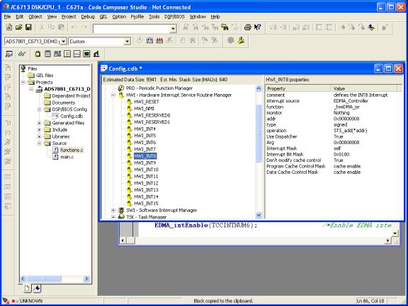
The sample application uses the DSP/BIOS utility of the CCS. This employs a GUI application to set up the timer, the EMIF/EDMA operation and interrupts. The GUI application takes care of setting up the control registers. The alternative to this is to set all this up manually using C code. TI documentation is thorough and this appears to be straight forward, but it looks like it would take considerable effort and time. I do not know which method yields the most efficient code. A screen shot of the DSP/BIOS tool is shown in Appendix A, Figure A2.
A block diagram of the interface from the reference TI Application Report is shown in Figure 7. In a nutshell, the DSP ‘C6713 Timer 1 initiates sampling by the ADS7881 on a rising pulse. As the ADS7881 is making an A to D conversion, the BUSY pin goes high. When the BUSY pin goes low, an interrupt is sent to the Enhanced Direct Memory Access (EDMA) controller, which in turn initiate a data read from address 0xA0014000. This address mapping enables the /RD pin of the ADS7881 and data can then be read on the External Memory InterFace (EMIF) data bus. The EDMA controller then writes the data to the DSK’s on board RAM.
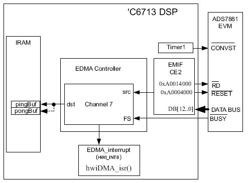
Figure 7 – Block Diagram of ADC – DSK Interface The EDMA Controller reads data from the ADS7881 via the EMIF. It then writes the data to the DSK ram. Timer 1 sets the sample rate of the ADS7881. The /BUSY signal triggers a data read. This figure is taken from Interfacing the ADS7881 to the TMS320C6713 DSP, Texas Instruments, http://focus.ti.com/lit/an/slaa257/slaa257.pdf
I go into a great level of detail here as I found it necessary to understand all of this to troubleshoot the interface and get it to work.
The control pins on the ADS7881 are designated as follows: (/ indicates “not” which means a low voltage activates it)
/CS – chip select
/RD – read
/CONVST – conversion start
BYTE – 8-bit or 12-bit bus
/PWDRST – reset
BUSY – performing conversion
These pins are brought out to J3 on the EVM. One side of J3 is tied to ground so that a jumper can be installed to tie any of these pins to ground. Pull-up resistors keep the pins high if not tied to ground except for the BUSY pin. For this application; /CS is shunted to ground so that the chip is always selected, and BYTE is shunted to ground indicating a 12 bit bus is used. Sampling is started on the rising edge of /CONVST. This means that the negative pulse that initiated a conversion is ending. This chip is designed so that even though an A to D conversion is taking place, a new sample can be taken. Obviously, there is a finite time needed for the conversion, so sample timing cannot exceed the rate at which conversion takes place. This sets the maximum sampling rate at 4MSPS. A timing diagram from the ADS7881 spec sheet is shown in Figure 8.
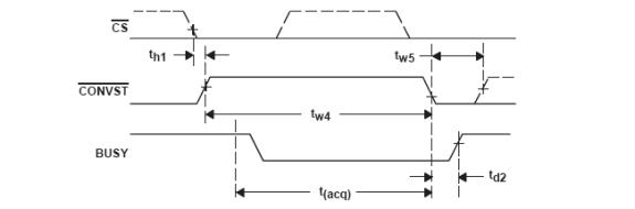
Figure 8 – ADS7881 Sample Start Timing. Sampling begins on falling edge of /CONVST. Taken from TI ADS7881 Datasheet http://focus.ti.com/lit/ds/symlink/ads7881.pdf
The /CONVST signal is produced by the ‘C6713 timer 1. Timer 1 derives its timing from an integer division of the 225 MHz clock that runs the ‘C6713. This is set up using the DSP/ BIOS. The DSP/BIOS settings are stored in a text file that is created by a GUI application within the CCS. This file was already created in the sample application. I will provide details on creating this file when I explain how I created mine for the AM_Radio project. A screen shot of the timer configuration is shown in Appendix A, Figure A3.
The Period Register (PRD) contains the hex value that determines the timer rate. Since 0x0000000E in Hex is 14 decimal, the timer rate is derived as follows:
![]()
The Timer 1 signal leaves the DSK on pin 49 of J3 and ends up on pin 3 on P2 on the EVM. This pin is wired to the center on of W2 and makes its way to /CONVST.
Data is read from the ADC to what is referred to as a ping-pong buffer. The general idea here is that while data is being written to the ping buffer, the DSP is reading from the pong buffer, and then data is written to the pong buffer while the DSP reads from the ping buffer. Data is read from the ADC by the DSP’s Enhanced Direct Memory Access (EDMA) and written to the onboard DSK memory. The EDMA is set up into channels. Channel 7 is used for this application. There are two configurations for channel 7 used, edmaCfgChan7 and edmaCfgChan7A. Configuration edmaCfgChan7 writes to an array pingBuf[] and edmaCfgChan7A writes to pongBuf[]. These configurations for channel 7 are linked, which means that the first time that channel 7 is activated, channel 7 uses edmaCfgChan7, and the next time it uses edmaCfgChan7A. Figures A7-A9 in Appendix A show how to set this up. An EDMA channel is activated by an EDMA event. The default event for EDMA channel 7 is hardware interrupt 7.
Interrupt 7 is set by the falling edge of the BUSY signal on the ADS7881. This negative going pulse is turned into a positive going pulse by the jumper W4 on the EVM (/BUSY) and proceeds to pin 1 on P2. This ends up on pin 68 or J3 on the DSK, which is hardware, interrupt 7. When this EDMA event occurs, it reads from the data bus and writes to either pingBuf[] or pongBuf[], depending on which configuration is used. Data is read from the ADC when the /RD pin is low. The /RD is wired to pin 10 (Y5) of a 3 to 8 decoder on the EVM board. It is a SN74AHC138. The function table for the SN74AHC138 is shown in Figure 9.
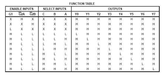
Figure 9 – SN74AHC138 Function Table Taken from TI SN74AHC138 Datasheet http://focus.ti.com/docs/prod/folders/print/sn74ahc138.html
As can be seen, for Y5 to be low, the inputs A, B, and C need to be 101. A, B, and C, are hardwired to DSK address lines A14, A15, and A16. Note that the shunt must be removed from W1 on the 5-6K interface board to set this. The binary address is then 10100000000000000. This is 0x14000 hex. The EMIF CE2 block of memory is used here which starts at 0xA0000000. The address mapping to set the /RD pin low is then 0xA0014000. The screen for setting up this source address for edmaCfgChan7 is shown in Appendix A Figure A4. When the EDMA reads from this address, /RD is set low and the ADC writes data to the data bus.
The EDMA configuration edmaCfgChan7 writes to the array pingBuf[]. The screen for setting up this destination address is shown in Appendix A, Figure A5.
When the EDMA configuration is finished writing to each element of array pingBuf[] or pongBuf[], it generates an interrupt to the DSP. The default EDMA interrupt is interrupt 8, which is used here. Interrupt 8 is set to run an Interrupt Service Routine (ISR), hwiDMA_isr(), which is a C function that resides in the file functions.c. The ISR is ahown in Listing D1 in Appendix D. The interrupt service routine is mapped to interrupt 8 by the DSP/BIOS as shown in Appendix A, Figure A6. The code that transfers the samples from the arrays filled by the EDMA to the arrays to be used by the application is shown here:
if (pingpong==1){
EDMA_disableChannel(hEdmaCha7);
/*Disable EMDA channel 7 -RD#*/
TIMER_pause(hTimer1);
for(i=0;i<BLOCK_SZ;i++){
dataPing[i]=(pingBuf[i]
& 0x3FFC)>>2;
dataPong[i]=(pongBuf[i]
& 0x3FFC)>>2; //ADS7881 12-bit
word
}
}
pingpong++;
The first time that interrupt 8 to the CPU is sent, this routine skips over the if statement since pinpong = 0. The second time, both buffers are full and data is transferred to arrays dataPing[] and dataPong[]. Notice that the data from the buffer arrays is anded with 0x3FFC which is 11111111111100 in binary. As mentioned earlier, the ADS7881 is a 12-bit ADC and the EVM writes data to the data bus starting with bit 3. This and operation clears any extraneous data that may appear on other bits. The >>2 operation then bit shifts the data so that the first data bit is seen on bit one of the data bus.
Troubleshooting the Interface and Sample Application
The sample application would not compile initially. The following errors occurred “error: unrecognized cregister name 'FADCR', error: unrecognized cregister name 'FAUCR', error: unrecognized cregister name 'FMCR'”. I looked these up and found that they were unique to the ‘C6713. Adding -d"CHIP_6713" -mv6710 to the Build Options string to specify the chip solved the problem. I probably should have done this anyway. It also could not find two files it needed and I ended up just copying them into the directories where it was looking.
For trouble shooting the ADS7881 to ‘C6713 DSP interface, this one shot data read was not very useful. I first changed the Link Handle Table of edmaCfgChan7A to link back to edmaCfgChan7.
This way, interrupt 8 continuously bounces between the two configurations. Next I commented out some lines of code in hwiDMA_isr() to enable continuous operation. These are highlighted in Appendix D, Listing D2. The program will now continuously transfer samples to the data buffers and is suitable for troubleshooting purposes. Here is a brief summary of the major hardware problems I ran into getting the interface to work.
Problem
Solution
No signal on /CONVST Run jumper from EVM P2 pin 3 to center
pin of W2
No signal on BUSY Connect 5V to J2 of 5-6K interface card
No data read Fix bent pin 75 on J4 of ‘C6713 DSK
An oscilloscope trace of the 4MHz /CONVST signal and BUSY signal is shown in Figure 10. The /CONVST is the trace on the top. The pulse width is about 1.2 divisions at 0.2 microseconds per division.
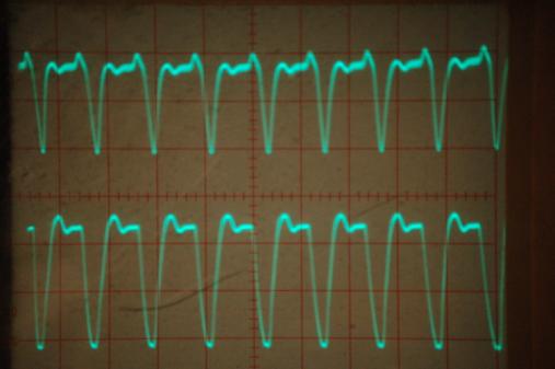
Figure 10 – Actual picture of Signal Traces of /CONVST and BUSY from my ‘C6713 DSK and ADS7881.
One could incorrectly conclude from this that the BUSY signal leads the /CONVST signal. What must be happening is that the conversion starts as the /CONVST signal is just starting to go in the negative direction.
The CCS has a view memory capability. This is how I determined that data was being read into the ‘C6713 DSK. Data in pingBuf[] hopefully indicates that the EDMA is reading valid data from the ADC and writing it to RAM. Data in dataPing[] shows that interrupt 8 is being serviced by the DSP. A screen shot is shown in Appendix A, Figure A10.
Software-defined AM Broadcast Radio Development
End-to-End Operation of the ADS7881 – ‘C6713 Configuration
At this point, I created my AM_Radio project. I copied code from the main.c and functions.c from the TI sample application to facilitate interfacing the ADS7881. I also created a new DSP/BIOS configuration file AM_Radio.cfg. This is straightforward, from the CCS Menu I chose File->New->DSP/BIOS Configuration. One then has to choose a “seed file”. I used the standard c6713.cdb. The CCS DSP/BIOS tool also creates AM_Radiocfg.cmd, which is why the file C6713dsk.cmd mentioned above is not used.
End to end operation includes integration of a codec into the application for audio output.
The ‘C6713 DSK uses a TI TLV320AIC23 stereo codec. Three files from Digital Signal Processing and Applications with the C6713 and C6416, by Rulph Chassaing are used to set up the codec; dsk6713_aic23.h, C6713dskinit.h, and C6713dskinit.c. Complete listings of these files can be found in Appendix E.
The ‘C6713 DSP includes two Multi channel Buffered Serial Ports (McBSPs) for serial interfacing. These are used to interface with the AIC23 codec. McBSP0 is used for control signals to the AIC23 and McBSP1 is used to read and write data. The header file dsk6713_aic23.h sets up handles to the AIC23 and McBSPs. It also provides parameters to set up the registers for the AIC23.
The file C6713dskinit.c contains the functions c6713_dsk_init(), comm_intr(), and output_sample(). The function c6713_dsk_init() initializes the AIC23 codec and McBSPs. The function comm_intr() does housekeeping to process the interrupt from the McBSP when it ready to receive a sample for output, and output_sample() provides the sample to the McBSP which in turn sends it to the AIC23 codec. Functions c6713_dsk_init(), and comm_intr(), are called once from main() within AM_Radio.c and output_sample() is called from functions.c within the interrupt service routine that processes the McBSP interrupt. I have found that a sample must be ready when or shortly after this interrupt is set. I postulate that it needs to be sent before the next interrupt, which is timed by the sampling frequency. At any rate, if a sample is not sent in a timely manner, the whole ‘C6713 DSK locks up and must be reset.
To create an end-to-end application, I decided to initially run both the ADS7881 and the AIC23 codec at a sampling rate of 48KSPS. 48KSPS is one of the pre-set sampling rates for the AIC23. It is set by a line of code in AM_Radio.c which sets variable fs=DSK6713_AIC23_FREQ_48KHZ. DSK6713_AIC23_FREQ_48KHZ is defined as an integer, 6, in dsk6713_aic23.h. This is used by c6713_dsk_init() when it initializes the AIC23 codec. Setting up the ADS7881 for operation at the sampling rate was a little tricky. Using the formula used above,
![]()
I calculated the necessary ![]() or 0x494 hex.
or 0x494 hex.
When I entered this value into the newly created timerCfg1 properties however, data was not retrieved from the ADC. Looking at the /CONVST signal on the oscilloscope, I noticed that the pulse width was very small compared to the sampling time. The ‘C6713 timer can either run in pulse mode of clock mode. The TI Sample application running at 4MHz runs in pulse mode. Since clock mode produces a pulse that is 50% of the sampling time, I decided to try this. A screen shot for this is shown in Appendix A, Figure A11. Thankfully, this worked. However, running in clock mode cuts the sampling time in half. Therefore, the value I ended up using for the PRD was 1172/ 2=586 or 0x24A hex. This set up the timer to retrieve data at the 48KSPS rate.
The new interrupt service routine to service interrupt 8 from the EDMA is shown in Appendix D Listing D2. The code that toggles between the two data arrays is shown here:
if (pingpong==0)
{
for(i=0;i<BLOCK_SZ;i++)
{
dataPing[i]=((pingBuf[i]
& 0x3FFC)>>2; //ADS7881 12-bit
word
}
pingpong
= 1; //next EDMA dump to pong
}
else if(pingpong==1)
{
for(i=0;i<BLOCK_SZ;i++)
{
dataPong[i]=((pongBuf[i]
& 0x3FFC)>>2;
}
pingpong =
0; //next EDMA dump to ping
}
The first time this is called by EDMA configuration 7, pingpong =0 and the dataPing[] array is filled and pingpong is changed to 1. The second time it is called by EDMA configuration 7A, pinpong=1 and the dataPong[] array is filled. This goes back and forth continuously.
Interrupt 11 is mapped to the function hwiCodec_isr() by using the DSP/BIOS in the same manner as interrupt 8 was set. Appendix A, Figure A12 shows this. Listing D4 in Appendix D shows the interrupt service routing to service interrupt 11 from the McBSP. The code that writes samples to the McBSP is shown here:
if(count <
BLOCK_SZ)
{
output_sample(dataPing[count++]*gain);
//out with gain
}
else if(count
< 2 * BLOCK_SZ)
{
output_sample(dataPong[count++
- BLOCK_SZ]*gain);
}
if(count >= 2
* BLOCK_SZ)
{
count
= 0;
}
Here the variable count, initially at 0, is incremented to read successive data samples from dataPing[] and dataPong[]. The variable count is tested and if it is less than BLOCK_SZ, a sample from dataPing[] is sent to the MCBSP and then to the AIC23 codec by the output_sample() and count is incremented. The same process is used to output samples from dataPong[]. These arrays are next to each other in memory. The DATA_ALIGN directive shown in the statements below does this when the arrays are declared in AM_Radio.c. For this to work, BLOCK_SZ has to be a power of 2. By the way, the block size is defined in dc_conf.h. In this application, as in the TI sample application, it is set to 2048.
#pragma DATA_ALIGN(pingBuf,BLOCK_SZ);
#pragma
DATA_ALIGN(pongBuf,BLOCK_SZ);
#pragma DATA_ALIGN(dataPing,BLOCK_SZ);
#pragma DATA_ALIGN(dataPong,BLOCK_SZ);
I tried in vain to have a check in this routine to make sure that data had been read into the appropriate array, dataPing[] or dataPong[], before samples are sent to the codec. As far as I can determine, any significant delay in this routine will cause the ‘C6713 DSK to crash. I don’t know exactly how long from the setting of interrupt 11 that a sample needs to be written to the McBSP, but it seems that a holdup of a certain length will cause it to lock up. Perhaps it must get a sample before the next interrupt is ready to be set. This merits further investigation.
I used a Windows program, NCH Tone Generator, to produce sine waves for testing the end-to-end application. NCH Tone Generator can be downloaded from http://www.nch.com.au/tonegen/index.html. I made a connection from my computer’s sound card output to pin 2 of J2 on the ADS7881 EVM. The end-to-end application described above successfully reproduced a 1KHz sine wave from the output of the AIC codec.
AM
Rectification at 48KSPS48 Kilo Samples Per Second (KSPS)
To demodulate an AM signal, I use the C math function abs() to take the absolute value of the signal. This performs the envelope detection. To test this I included the header file math.h in the file functions.c, and added the abs() function to two lines of code in the ISR for interrupt 8 from the EDMA as shown below:
dataPing[i]=abs(((pingBuf[i]
& 0x3FFC)>>2)-0x7FF);
dataPong[i]=abs(((pongBuf[i] & 0x3FFC)>>2)-0x7FF);
The ADS7881 outputs 12 bit data from 0 to 4095. To demodulate an AM signal, this needs to be converted to data that represents a signal that goes evenly positive and negative, in other words, it has no DC component. The half way point for the maximum ADS7881 output, 4095, is 2047 or 0x7FF hex. This is why 0x7FF is subtracted from the data from pingBuf[] and pongBuf[] and then stored in a short signed integer. This required some adjustment of the input op amp on the ADS7881 EVM which I’ll explain a little later
When a 1KHz sine wave was input into the application, a sine wave came out, rather than a full wave rectified signal. The problem was with the input offset voltage setting on the ADS7881 EVM. The ADS7881 EVM provides for a DC offset voltage to the input analog signal that is controlled by a potentiometer, R25. Actually, this is really not a problem but rather an asset, since it provides control of this. First I removed the abs() function and the subtraction of -0x7FF from the data written to dataPing[]. I then I wrote a routine that averaged the values in dataPing[] and stored the average values in an array as shown below.
int
average;
short averageArray[1000]; // use short to save memory with
arrays
int count = 0;
….
for(i=0;i<BLOCK_SZ;i++)
{
dataPing[i]=((pingBuf[i]
& 0x3FFC)>>2); //ADS7881
12-bit
}
pingpong = 1; //next
EDMA dump to pong
average = 0; //zero out variable for new average
for (i=0; i< BLOCK_SZ; i++)
{
average +=
dataPing[i]; //add data to average
}
averageArray[count++]
= average/BLOCK_SZ; //calculate average
if(count >=
1000) // >= for safety
count
= 0; //zero counter to
start over
I also inserted a blocking capacitor in series with the signal path to remove any actual DC component. While running the application, I observed values in this array by the Quick Watch feature of CCS. This is accessed by the CCS menu View->Quick Watch. One can then enter the variable name in the window and see the value of the variable. Again, the12 bit output data from the ADS7881 varies between 0 and 4095, the halfway point being at 2047. I adjusted R25 until I got as close to an average of 2047 as possible. A screen shot is shown in Appendix A, Figure A13.
After restoring the abs() function and subtraction of 0x7FF to the code, the application successfully performed the rectification of the sine wave.
Figure 11 displays the a 1KHz input and the rectified output from the ‘C6713 DSK and AIC23 codec. Cannel 1 is the input and Channel 2 is the output. I am using a Windows program, OscilloMeter 6.0, to display this. This is an impressive application written by Oleg Ya. Shmelyoff that uses the computer’s sound card for I/O. It can be downloaded from http://shmelyoff.nm.ru. The free version runs for about 15 seconds and quits, but this is long enough for this purpose. The really impressive feature of this program is the spectrum analyzer and 3D spectrum analyzer that displays time on the z-axis. I also found the program to be a useful tool for filter design.
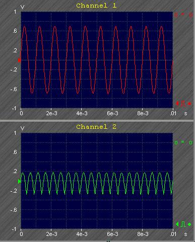
Figure 11 – Channel 1 shows incoming 1KHz signal generated by the host computer and input into the ADS7881. Channel 2 shows the ‘C6713 DSK’s codec output. This is the input signal run through the abs() function and thus rectified.
The OscilloMeter application also has a signal generator that can produce AM modulated signals. Figure 12 shows a 12KHz carrier modulated by a 100Hz sine wave on Channel 1. Channel 2 shows the output from the ‘C6713 rectifying application.
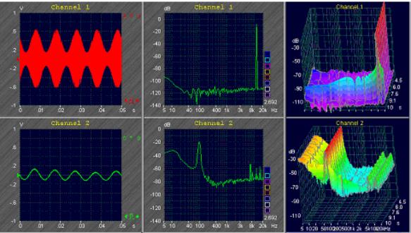
Figure 12 – Channel 1 shows the input 12KHz carrier modulated by a 100Hz sine wave. Channel 2 shows the rectified signal. The center windows show the spectral analysis of these signals. The windows on the right show the spectral analysis over time.
Initially, I was puzzled at the absence of the 12KHz carrier. Looking at the signal on an actual oscilloscope revealed a strong frequency component around 25KHz. It then occurred to me that the sine wave of the carrier frequency undergoes a full wave rectification that produces a signal with a period of half the original, resulting in the 25KHz (actually 24KHz) component. The computer sound card is not designed to pass a frequency of 24KHz and therefore, it is not observed by the application. To test this hypothesis, I modulated a 5KHz signal. Figure 13 demonstrates that the carrier component is indeed still there. Note here that the low frequency components are greatly reduced. Perhaps the 24KHz signal produced harmonics in the computer’s sound card that have these low fundamental frequencies.
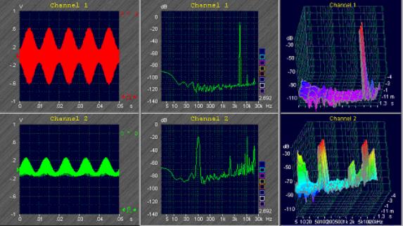
Figure 13 – Channel 1 shows the 5KHz modulated signal. Channel 2 shows the rectified signal with the carrier still present. The center and right windows show the spectral analysis of these signals.
Having successfully rectified an audio frequency AM signal, I proceeded to work on demodulation of an RF signal. Since I do not have an RF signal generator I decided to go ahead and actually use an AM Broadcast signal.
Antenna
Installation and Signal Discoveryrecovery
I ran about 50 ft. of #14 copper wire between two trees in my back yard for an antenna. Then I ran more of the same from the antenna through my basement window. Using a germanium diode and a small amplifier, I detected an AM station at 1120 KHz, WUST – New World Radio. The station’s website boasts that they broadcast in 17 different languages. Unfortunately, I have not found one that I understand, although I can listen to the music. The 20,000 watt transmitter and antenna are about 3.3 miles from my house. Since this one station comes in so strong, I decided that initially I would not use any type of tuned circuit and would attempt to directly demodulate the raw signal with the ‘C6713 DSP. An oscilloscope trace of the AM signal is shown in Figure 14.
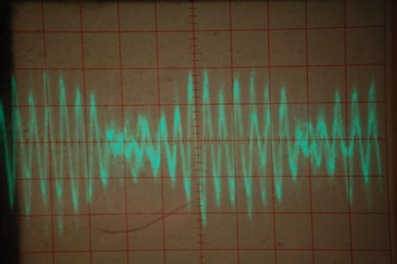
Figure 14 – Picture of oscilloscope trace of actual AM Signal from WUST 1120 KHz
The sweep time is set at 2 microseconds per division. This looks like one can see the message modulation, however, at 2 microseconds per division, the modulating signal would be about 100 KHz. The vertical scale is set at 0.2 Volts per division, yielding a maximum voltage of 0.8 Volts. With the signal conditioning on the ADS7881 EVM, this is within the acceptable range of input, so I will connect the antenna directly to pin 2 of P1 on the EVM board.
Realization of the Working AM Broadcast DSP Radio
Listings of the files used in the AM Radio application are found in Appendix C. Processing the AM Broadcast signal requires sampling the RF signal at a relatively high rate around 3.2 MSPS, and then converting the data samples to run the lower sampling rate of the AIC23 codec. The codec has fixed sampling rates of 8, 16, 24, 44.1, 48, and 96 KHz. To make this conversion, a sample is extracted from the higher rate samples every n samples. To find an appropriate value for n, I made up the spreadsheet shown in Figure 26. The numbers in the spreadsheet in the columns below the AIC23 sample rates are possible values of n. Remember that the Timer 1 rat is set by the formula:
![]()
Since the Timer 1 rate is determined by an integer divisor, and the AIC23 has fixed sampling rates, there is no exact match. I chose to pick a value for n that is a power of 2 so that there are an exact number of sample extractions for each BLOCK_SZ. By trial and error, I found this to work best. After much experimentation, I settled on an n of 64 with Timer 1 at 3.125 MHz, and the AIC23 sampling rate at 48 KSPS. Since the calculated value of n is 65.104, there should be slightly more samples available for extraction than a perfect match. For a perfect match for an n of 64, the Timer 1 rate would be 64 x 48,000 = 3.072 MHz.
I set the new rate of Timer 1 to 3.125 MHz by entering a PRD of 18, 0x12 hex, in the DSP/BIOS as shown in the previous example. Leaving the EDMA interrupt ISR for interrupt 8 as is, I modified the McBSP ISR for interrupt 11 for the 1 in 64 sample extraction as shown in Appendix D Listing D5. The code that does the extraction is shown below:
if(count <
BLOCK_SZ)
{
output_sample(dataPing[count]*gain);
//out with gain
}
else if(count
< 2 * BLOCK_SZ)
{
output_sample(dataPong[count
- BLOCK_SZ]*gain);
}
count += 64;
if(count >= 2
* BLOCK_SZ)
{
count
= 0;
}
Here I no
longer increment the variable count in the array index and increment it by 64
in a separate statement. Loading this program into the ‘C6713 DSP, connecting
the antenna to the input of the ADS7881 EVM, and connecting the AIC23 output to
amplified speakers, I could hear an audio output that contained intelligence
from the AM signal. However, with just the rectification, the intelligence is
hard to identify and there are frequencies present that are probably caused by
aliasing. In order to develop a listenable radio, a low pass filter is required
after the rectification.
I used the program MATLAB to design an FIR lowpass filter. MATLAB has a filter designer called fdatool. Appendix B, Figure B1 shows a screen shot of this. An ideal lowpass filter would completely stop frequencies at twice the highest message frequency and higher. Since the bandwidth of an AM signal is 5KHz, this would mean that frequencies of 10KHz and higher would be blocked. However, since the ratio of the ideal stop frequency (ideally 10 KHz) to the frequency of the sampling rate, 3 MHz, is so great, I had to compromise quite a bit to get a realizable filter. As can be seen, the pass frequency is set at 10 KHz and the stop frequency is set at 60 KHz. After experimenting with various filters, this one proved to work quite well. I set the order at 60 to facilitate the implementation of the filter, as I will explain shortly.
I used the method that Rulph Chassaing uses in his book Digital Signal Processing and Applications, to implement this filter. The coefficients exported to the MATLAB workspace are in floating point format and stored in a variable array Num. They are converted to integers by performing the following operation in the MATLAB workspace:
EDU>> round(Num * 2^15);
I then
cut and pasted the coefficients into a header file, lp10k.h. A listing of this
file is found in Appendix C. This file sets up an array h[] that contains the
filter coefficients. The filter is implemented by the following lines of code:
yn = 0; //initialize filter's output
for (i = 0; i< N; i++)
yn += (h[i] * dataPing[i]); //y(n) += h(i)* x(n-i)
outBuf[dataCount++] = yn >> 15; //write
filtered data to output buffer
/* end FIR filter */
I have created an array, outBuf[], to store the filtered data. I experimented with doing away with the ping pong arrangement, since the output is essentially free running. The samples are either there or they aren’t. However, for some reason, the using only one EDMA configuration only wrote samples to outBuff[] at a rate half of that required. I actually tried cutting the AIC23 sampling rate in half to 24 KBPS. This worked, but the sound quality was not as good as the original arrangement. Rather than trying to force the issue, I simply retained the ping pong procedure.
I pull a trick in implementing the lowpass filter. Normally, each individual sample is filtered by entering the filter coefficients into a difference equation with the preceding N samples. To do this, and array needs to be set up in which either the contents of the array are shifted back one place for each new sample, or a circular buffer is used in which a pointer index is shifted for each new sample. In this case, however, only one sample is needed for output from every 64 input samples. By limiting the order of the FIR filter to 60, I can simply use the samples in the dataPing[] or dataPong[] array for the difference equation and get the one sample needed for output. The bit shifting >>15 compensates for the fixed-point coefficient manipulation done in MATLAB.
The ISR for the McBSP interrupt 11 simply sends samples from outBuf[] to the McBSP and on to the AIC23 as shown in the following lines of code:
output_sample(outBuf[outCount++]*gain);
if(outCount >= 8000)
{
outCount = 0;
}
The application now demodulates the AM broadcast signal and produces an acceptable audio output. Figure 15 shows the AM signal from the antenna and the demodulated audio output.
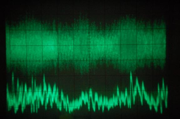
Figure 15 – Picture of oscilloscope traces of actual input and output signals from the AM Software-defined radio. The AM signal from the antenna is on the top and the audio output from the ‘C6713 DSK is on the bottom. The horizontal axis is set at 1 millisecond per division.
Results
This project demonstrates that it is possible to build an AM Broadcast demodulator with a ‘C6713 DSP and a ADS7881 Analog to Digital converter. The demodulator uses the C programming math function, abs(), to perform a rectifying action in software that emulates a hardware rectification with a diode. A lowpass FIR filter is then implemented to remove alias frequencies. The result was a working AM receiver.
You can hear a .wav file of the raw rectified signal and
alias interference at the following link:
http://bill.rideout.com/AM_Rectified.wav
A recording of the demodulated and filtered output is here:
http://bill.rideout.com/AM_Demod.wav
Many DSP textbooks have AM demodulation examples, but all I have seen operate at audio frequencies. While these are informative as to the programming capabilities of the particular DSP, they do not address many of the problems encountered in building an actual radio receiver. One issue that I have not addressed in any of these examples is the problem of sampling at a relatively high rate and then outputting an audio signal at a lower sampling rate. In this particular exercise, two separate clocks were used for the respective sampling rates. If a receiver were built from scratch, many of the problems I encountered could be solved by using a single clock to derive both sampling rates. I did not have ability to do this with the resources at hand. Another issue is the lowpass filter. It is relatively painless to design a lowpass filter when the ratio of cutoff frequency to sampling frequency is relatively large but much more difficult when these frequencies are as far apart as in this project.
This was a tremendous learning experience for me. I have found that real time programming can be quite challenging. Initially, I had envisioned including a tuner to select frequencies, and also demonstration of various demodulation techniques. This would more clearly demonstrate the benefits of Software Defined Radio. As it turned out, I spent much time becoming familiar with the ‘C6713 DSP and real time programming in general. Setting up the ADS7881 also took much more time and effort than I had planned on. I hope that the documentation here may be helpful to others attempting this endeavor.
Summary and Conclusions
This project demonstrated that a working software defined Broadcast AM demodulator can be built with a TI TMS320C6713 DSP and a TI ADS7881 Analog to Digital converter. More importantly, it documented the effort required to do so. One could argue that a 50 cent Germanium diode, a resistor and capacitor can perform the same function. However, it is good to have a baseline on the effort required to build a simple receiver in software, to help in the decision process of whether to go with a software or hardware design for a more sophisticated radio.
I can think of two situations where a Software Designed Radio makes sense, even for a simple envelope detector. There is no local oscillator, even if a full tuner is implemented in software. This means that a radio receiver could operate undetected as it would not broadcast any signal from the local oscillator. Another instance is if the radio was part of a receiver that used different modulation schemes that could be changed in software as needed.
I personally found this project to be interesting and rewarding. I learned much about DSP and real time programming, specifically focusing on the TMS320C6713 DSP. I also learned much about data conversion. In many instances in the software application, I went with what worked rather than with what would be a more elegant solution. For instance, the output does not have any check that the data samples are ready. Conversely, the input sampling has no mechanism to stop it from overwriting data before it is processed. It seems that the ‘C6713 DSK’s serial output buffer, the McBSP, is quite sensitive to having a routine of great length to service its interrupt. I came to the conclusion that trying to hold up the output was a dead end. My next approach was to run the input sampling at a slightly higher rate and then periodically disable it to wait for the output to catch up. Researching this indicated that sampling rate used; disabling either Timer 1, the source of the sampling signal, or disabling the EDMA channel, takes a relatively long time and that samples would still be taken and written to memory after this was initiated. At any rate, the rates match up well enough to provide a reasonable audio output. The next step is to implement some type of software tuning functionality. This probably would involve a Phase Lock Loop implementation and would provide a more useful radio.
I have tried to thoroughly document my effort here. Hopefully this can be a resource for someone attempting a similar endeavor either in TMS320C6713 DSP implementation or even just getting the ADS7881 EVM board working.
References
Digital Signal Processing and Applications with the C6713 and C6416 DSK, Chassing, Rulph, 2005, John Wiley and sons.
Communication System Design Using DSP Algorithms, Tretter, Steven A., 2003 Springer Science+Business Media, Inc.
TMS320C6713 DSK Technical Reference, Spectrum Digital/ Texas Instruments. http://c6000.spectrumdigital.com/dsk6713/V1/docs/dsk6713_TechRef.pdf
Interfacing the ADS7881 to the TMS320C6713 DSP Application Report SLAA257, July 2005 Texas Instruments. http://focus.ti.com/lit/an/slaa257/slaa257.pdf
5-6K Interface Board User’s Guide SLAU104B, May 2004-Revised May 2006 Texas Instruments http://focus.ti.com/lit/ug/slau104b/slau104b.pdf
ADS7881/ADS7891 EVM User’s Guide SLAU150, December 2004 Texas Instruments. http://focus.ti.com/lit/ug/slau150/slau150.pdf
ADS7881 SLAS400B, September 2003 – Revised November
2005 Texas Instruments
TMS320C6000
Peripherals Reference Guide SPRU190D, February 2001 Texas Instruments. http://focus.ti.com/lit/ds/symlink/ads7881.pdf
Software Defined Radio, http://en-wikipedia.org/wiki/Software-defined_radio
Appendices
Appendix A - Code Composer Studio Screen Shots
This appendix shows screen shots from the Texas Instruments Code Composer Studio that comes with the TMS320C6713 DSK. These are representations of the actual windows.
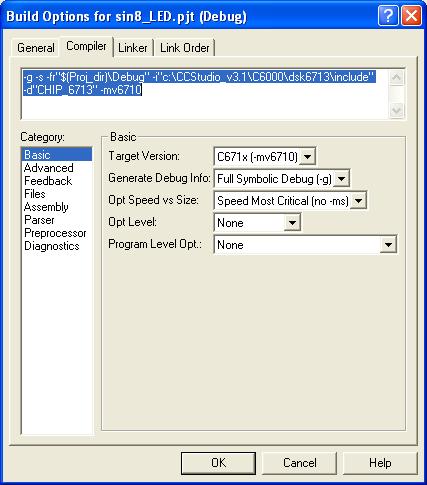
Figure A1 – Window that shows the addition of an include path to Build Options. This screen is accessed from the CCS’s menu item Project->Build Options.
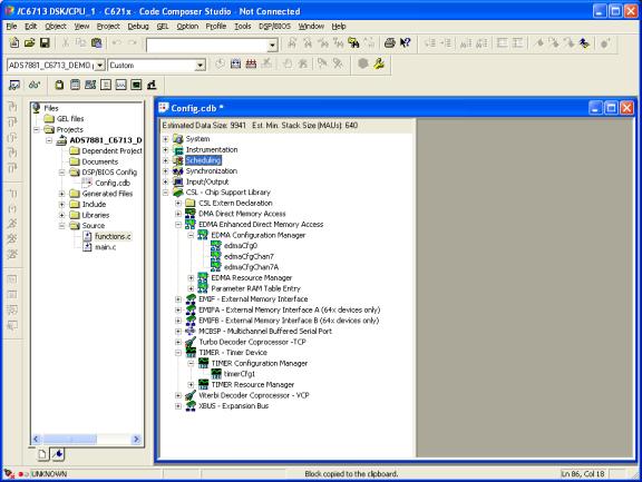
Figure A2 – Screen shot of DSP/BIOS Configuration. This is accessed by clicking on Config.cdb from the DSP/BIOS section of the Project Tree.
![]()
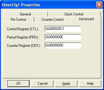
Figure A3 –
Setting Timer 1 in the DSP/BIOS. PRD value = ![]()
![]()

Figure A4 – Setting the Source Address for edmaCfgChan7
![]()
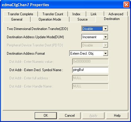
Figure A5 – Setting the Destination Address for edmaCfgChan7
![]()
Figure
A6 – Setting Interrupt Mapping in DSP/BIOS
![]()
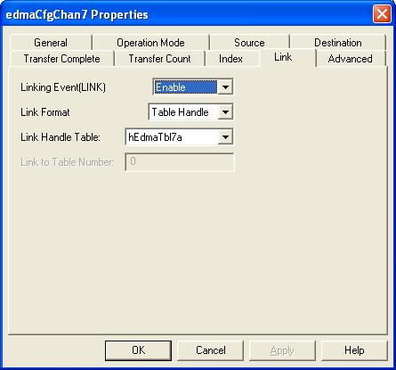
Figure A7 –
Setting up the Link Handle Table Setting for edmaCfgChan7
![]()
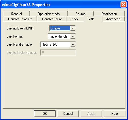
Figure A8 –
Setting up the Link Handle Table Setting for edmaCfgChan7A
![]()

Figure A9 – New
Link Setting for edmaCfgChan7A
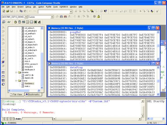
Figure A10 – View of DSK
ram showing valid data in pingBuf[] and demonstrating that the ISR has
successfully run and written data to dataPing[].
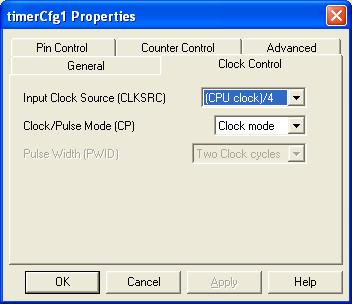
Figure A11 –
Setting Timer 1 for Clock Mode
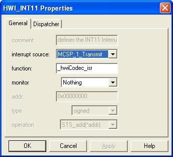
Figure A12 – Mapping Interrupt 11 to ISR
 .
.
Figure A13 – Average of dataPing[], the goal was to get the average to 2047.
Appendix B – MATLAB Screen Shots
The following are representations of windows form the MATLAB fdatool.
Figure B1– Lowpass Filter Design with fdatool. Some compromises were made since Fstop << Fs
Figure B2 – Window
showing how to export coefficients to MATLAB Workspace The filter
coefficients can be exported to the MATLAB workspace by using the menu item
File->Export.
Appendix C – Listings of AM_Radio.c, functions.c, and lp10k.h
AM_Radio.c
//Program to demodulate AM signal
/* The skeleton for this file is taken from main.c from the sample
applocation
described in Interfaceing the ADS7881 to the TME320C6713 DSP
form Texas Insturments available at
http://focus.ti.com/analog/docs/tech
*/
#include "AM_Radiocfg.h" //generated support file
#include "dsk6713.h"
#include "dsk6713_led.h"
#include "dsk6713_dip.h"
#include "dsk6713_aic23.h" //codec-DSK
support file
Uint32 fs=DSK6713_AIC23_FREQ_48KHZ;
//set
sampling rate
/* Include Header
File */
#include "dc_conf.h"
/* include files for DSP/BIOS */
#include <std.h>
#include <swi.h>
#include <log.h>
/* include files for chip support library */
#include <csl.h>
#include <csl_legacy.h>
#include <csl_irq.h>
#include <csl_timer.h>
#include <csl_edma.h>
/* function prototypes */
void init_dsk(void);
/* Create the buffers. We want to align the buffers to be cache
friendly */
/* by aligning them on an L2 cache line boundary.
*/
#pragma DATA_ALIGN(pingBuf,BLOCK_SZ);
#pragma DATA_ALIGN(pongBuf,BLOCK_SZ);
#pragma DATA_ALIGN(dataPing,BLOCK_SZ);
#pragma DATA_ALIGN(dataPong,BLOCK_SZ);
unsigned short pingBuf[BLOCK_SZ];
/*data from AD, written to by EDMA
*/
unsigned short pongBuf[BLOCK_SZ];
/*data from AD, written to by EDMA
*/
short dataPing[BLOCK_SZ];
/*data from AD, written to by EDMA
*/
short dataPong[BLOCK_SZ];
/*data from AD, written to by EDMA
*/
void main()
{
int i;
comm_intr();
//Set up communication with codec via McBSP
/* initialize the
EMIF*/
init_dsk();
IRQ_reset(IRQ_EVT_EDMAINT); /*Reset
EDMA interrupt */
IRQ_clear(IRQ_EVT_EXTINT7);
TIMER_reset(hTimer1);
for (i=0; i<=BLOCK_SZ; i++) { /*Initialize data buffers */
pingBuf[i]=0x00000;
dataPing[i]=0x00000;
pongBuf[i]=0x00000;
dataPong[i]=0x00000;
}
/* Enable the EDMA controller interrupt */
IRQ_enable(IRQ_EVT_EDMAINT);
EDMA_intDisable(TCCINTNUM6); /*Disable
EDMA interrupt */
EDMA_intClear(TCCINTNUM6); /*Clear
EDMA interrupt */
EDMA_intEnable(TCCINTNUM6); /*Enable EDMA interrupt */
/*Configuration of Timer1 and EDMA channel 7 */
EDMA_config(hEdmaCha7,&edmaCfgChan7);
TIMER_config(hTimer1,&timerCfg1);
EDMA_clearChannel(hEdmaCha7);
/*Only Timer1 and Edma Channel 7*/
EDMA_enableChannel(hEdmaCha7); /*Enable EDMA channel 7 -RD# */
TIMER_start(hTimer1); /*Start
A/D CONVST# trigger */
}
functions.c
//functions.c Initialization functions and interrupt service
// routines for AM_Radio project
/*
The skeleton for this file is taken from the sample application
described in Interfaceing the ADS7881 to the TME320C6713 DSP
form Texas Insturments available at
http://focus.ti.com/analog/docs/techdocsabstract.tsp?familyId=390&abstractName=slaa257
*/
/* Include Header
File */
#include "AM_Radiocfg.h"
#include "dc_conf.h"
#include <csl_legacy.h>
#include <math.h>
#include "lp10k.h"
extern unsigned short pingBuf[BLOCK_SZ]; // arrays to store EDMA
samples
extern unsigned short pongBuf[BLOCK_SZ];
extern short dataPing[BLOCK_SZ];
extern short dataPong[BLOCK_SZ];
int pingpong = 0;
//variable to toggle between ping and pong
short outBuf[8000]; // array to store ouput samples
int dataCount = 0; //
counter variable used by EDMA ISR
int outCount = 0;
//counter variable used by McBSP ISR
int i;
short dly[N];
int yn =0;
int gain = 30; // multiplier to increase output volume
//void stageTwo();
/****************************************************************/
/* init_dsk()
*/
/* This initializes the EMIF */
/****************************************************************/
void init_dsk(void)
{
UINT32
gblctl,ce0ctl,ce1ctl,ce2ctl,ce3ctl,sdctl,sdtim,sdext;
/* intialization of the
EMIF */
/* RBTR8,SSCRT,CLK2EN,CLK1EN,SSCEN,SDCEN,NOHOLD */
gblctl =
EMIF_MK_GBLCTL( 0, 0, 1, 0, 0, 0, 0);
/*
RDHLD,MTYPE,RDSTRB,TA,RDSETUP,WRHLD,WRSTRB,WRSETUP */
ce0ctl = EMIF_MK_CECTL(
0, 3, 0, 0, 0, 0, 0, 0);
/* RDHLD,MTYPE,RDSTRB,TA,RDSETUP,WRHLD,WRSTRB,WRSETUP
*/
ce1ctl = EMIF_MK_CECTL(
0, 2, 0, 0, 0, 0, 0, 0);
/*
RDHLD,MTYPE,RDSTRB,TA,RDSETUP,WRHLD,WRSTRB,WRSETUP */
ce3ctl = EMIF_MK_CECTL(
0, 2, 0, 0, 0, 0, 0, 0);
/*
TRC,TRP,TRCD,INIT,RFEN,SDWID,SDCSZ,SDRSZ,SDBSZ */
sdctl = EMIF_MK_SDCTL(
7, 1, 1, 1, 1, 0, 1, 0, 0);
/* PERIOD,XRFR */
sdtim =
EMIF_MK_SDTIM( 1562, 0);
sdext = EMIF_SDEXT_NA;
/* make CE2 control
register value */
/* This is the CE space
used by the ADS8402 EVM. */
/* Use the timing
values from dc_conf.h: */
ce2ctl = EMIF_MK_CECTL(
EMIF_CECTL_RDHLD_OF
(RDHLD), /* read hold
*/
EMIF_CECTL_MTYPE_ASYNC32,
EMIF_CECTL_RDSTRB_OF
(RDSTRB), /* read strobe */
EMIF_CECTL_TA_NA,
EMIF_CECTL_RDSETUP_OF (RDSETUP),
/* read setup */
EMIF_CECTL_WRHLD_OF
(WRHLD), /* write hold */
EMIF_CECTL_WRSTRB_OF
(WRSTRB), /* write strobe */
EMIF_CECTL_WRSETUP_OF
(WRSETUP) /* write setup */
);
/* configure the EMIF
*/
EMIF_ConfigB(gblctl,ce0ctl,ce1ctl,ce2ctl,
ce3ctl,sdctl,sdtim,sdext);
return;
} /* end init_dsk() */
/*
* hwiDMA_isr - interrupt service routine to service interrupt 8
from EDMA
* channel 7
*/
void hwiDMA_isr()
{
int i;
if (pingpong==0)
{
for(i=0;i<BLOCK_SZ;i++)
{
dataPing[i]=abs(((pingBuf[i]
& 0x3FFC)>>2)-0x7FF); //ADS7881 12-bit
}
/*
FIR lowpasss filter */
yn =
0; //initialize
filter's output
for
(i = 0; i< N; i++)
yn
+= (h[i] * dataPing[i]); //y(n) +=
h(i)* x(n-i)
outBuf[dataCount++]
= yn >> 15; //write filtered data to output buffer
/*
end FIR filter */
pingpong = 1; //next EDMA dump to pong
}
else
if(pingpong==1)
{
for(i=0;i<BLOCK_SZ;i++)
{
dataPong[i]=abs(((pongBuf[i] &
0x3FFC)>>2)-0x7FF);
}
/*
FIR lowpasss filter */
yn =
0; //initialize
filter's output
for (i
= 0; i< N; i++)
yn
+= (h[i] * dataPong[i]); //y(n) +=
h(i)* x(n-i)
outBuf[dataCount++]
= yn >> 15;
/*
end FIR filter */
pingpong = 0;
}
if(dataCount
>= 8000)
{
dataCount
= 0;
}
IRQ_reset(IRQ_EVT_EDMAINT); /*Reset EDMA interrupt */
IRQ_enable(IRQ_EVT_EDMAINT);
EDMA_intDisable(TCCINTNUM6); /*Disable
EDMA interrupt */
EDMA_intClear(TCCINTNUM6); /*Clear
EDMA interrupt */
EDMA_intEnable(TCCINTNUM6); /*Enable EDMA interrupt */
}
/*
* hwiCodec_isr - interrupt service routine for interrupt 11 from
McBSP
*/
interrupt void hwiCodec_isr()
{
output_sample(outBuf[outCount++]*gain);
if(outCount >=
8000)
{
outCount
= 0;
}
}
/****************************************************************/
/* End Functions.c
*/
/****************************************************************/
lp10k.h
/*bp12m.cof FIR bandpass filter coefficients file*/
#define N 61
/*length of filter*/
short h[N]=
{
851, 202, 225,
248, 272, 297,
322, 348, 374,
400, 427,
453, 479, 504,
529, 553, 576,
599, 620, 640, 659,
677,
693, 707, 719,
731, 739, 746,
751, 755, 756,
755, 751,
746, 739, 731,
719, 707, 693,
677, 659, 640,
620, 599,
576, 553, 529,
504, 479, 453,
427, 400, 374,
348, 322,
297, 272, 248,
225, 202, 851
};
Appendix D – Evolution of Interrupt Service Routines
int
pingpong=0; /*=1 pingbuffer full*/
void hwiDMA_isr()
{ int i;
if (pingpong==1){
EDMA_disableChannel(hEdmaCha7);
/*Disable EMDA channel 7 -RD#*/
TIMER_pause(hTimer1);
for(i=0;i<BLOCK_SZ;i++){
dataPing[i]=(pingBuf[i]
& 0x3FFC)>>2;
dataPong[i]=(pongBuf[i]
& 0x3FFC)>>2; //ADS7881 12-bit
word
}
}
pingpong++;
IRQ_reset(IRQ_EVT_EDMAINT); /*Reset EDMA interrupt */
IRQ_enable(IRQ_EVT_EDMAINT);
EDMA_intDisable(TCCINTNUM6); /*Disable EDMA interrupt */
EDMA_intClear(TCCINTNUM6) ; /*Clear
EDMA interrupt */
EDMA_intEnable(TCCINTNUM6); /*Enable EDMA interrupt */
}
Listing D1 – Original Interrupt Service
Routine from
the TI application found at http://focus.ti.com/analog/docs/techdocsabstract.tsp?familyId=390&abstractName=slaa2
57 When the
EDMA fires interrupt 8, data is transferred to dataPing[] and dataPong[].
void hwiDMA_isr()
{ int i;
//if (pingpong==1){
// EDMA_disableChannel(hEdmaCha7);
/*Disable EMDA channel 7 -RD#*/
// TIMER_pause(hTimer1);
for(i=0;i<BLOCK_SZ;i++){
dataPing[i]=(pingBuf[i]
& 0x3FFC)>>2;
dataPong[i]=(pongBuf[i]
& 0x3FFC)>>2; //ADS7881 12-bit
word
// }
}
// pingpong++;
IRQ_reset(IRQ_EVT_EDMAINT); /*Reset EDMA interrupt */
IRQ_enable(IRQ_EVT_EDMAINT);
EDMA_intDisable(TCCINTNUM6); /*Disable EDMA interrupt */
EDMA_intClear(TCCINTNUM6); /*Clear
EDMA interrupt */
EDMA_intEnable(TCCINTNUM6); /*Enable EDMA interrupt */
}
Listing D2– The if statement is removed so that the ISR will continually write to the data arrays.
void hwiDMA_isr()
{ int i;
if (pingpong==0)
{
for(i=0;i<BLOCK_SZ;i++)
{
dataPing[i]=((pingBuf[i]
& 0x3FFC)>>2; //ADS7881
12-bit word
}
pingpong
= 1; //next EDMA dump to pong
}
else if(pingpong==1)
{
for(i=0;i<BLOCK_SZ;i++)
{
dataPong[i]=((pongBuf[i]
& 0x3FFC)>>2;
}
pingpong =
0; //next EDMA dump to ping
}
IRQ_reset(IRQ_EVT_EDMAINT); /*Reset EDMA interrupt */
IRQ_enable(IRQ_EVT_EDMAINT);
EDMA_intDisable(TCCINTNUM6); /*Disable EDMA interrupt */
EDMA_intClear(TCCINTNUM6); /*Clear EDMA interrupt */
EDMA_intEnable(TCCINTNUM6); /*Enable EDMA interrupt */
}
Listing D3 – ISR for Interrupt 8 for End to End Application. EDMA toggles writes between dataPing[] and dataPong[]/
interrupt void hwiCodec_isr()
{
if(count <
BLOCK_SZ)
{
output_sample(dataPing[count++]*gain);
//out with gain
}
else if(count
< 2 * BLOCK_SZ)
{
output_sample(dataPong[count++
- BLOCK_SZ]*gain);
}
if(count >= 2
* BLOCK_SZ)
{
count
= 0;
}
}
Listing D4 – ISR for Interrupt 11. Samples are written to the AIC23 codec via the McBSP buffer
interrupt void hwiCodec_isr()
{
if(count <
BLOCK_SZ)
{
output_sample(dataPing[count]*gain);
//out with gain
}
else if(count
< 2 * BLOCK_SZ)
{
output_sample(dataPong[count
- BLOCK_SZ]*gain);
}
count += 64;
if(count >= 2
* BLOCK_SZ)
{
count
= 0;
}
}
Listing D5 – ISR for Interrupt 11 for RF
Rectification. The variable count is incremented by 64 to only extract each 64th
sample.